rf-low-pass-filter-design-specs-and-applications, rf-low-pass-filter-design-specs-and-applications, /news
Inquiry
Inquiry

RF Low Pass Filter: Design, Specs and Applications

2026/09/07

RF Low Pass Filter: Design, Specs and Applications

Engineers working on modern wireless systems constantly struggle with unwanted harmonics, out‑of‑band emissions, and cross‑channel interference. An RF low pass filter serves as a fundamental line of defense in the RF front‑end. Its core job is simple: let signals below a target cutoff frequency pass with minimal attenuation while heavy‑handed attenuation blocks higher frequencies. However, translating that simple concept into reliable hardware requires balancing insertion loss, power handling, package size, and phase response.

Selecting the right RF low pass filter geometry and dialing in specifications directly determines whether a system achieves regulatory compliance and robust link margins. Understanding these trade‑offs is essential for designing modern telecom base stations, IoT modules, and broadcast transmitters.

Understanding Core Filter Topologies

Choosing an RF low pass filter requires selecting the right physical topology for your operating frequency, power requirements, and mechanical design limits. The three main physical choices in RF design are lumped‑element LC filters, ceramic RF filters, and high‑power cavity low pass filters.

  • Lumped‑Element LC Filters: Standard inductors and capacitors work well for low‑frequency designs up to roughly 1 GHz. Their primary advantage lies in layout flexibility, low initial cost, and easy tuning of cutoff frequencies. However, at higher microwave frequencies, parasitic capacitance, series inductance, and component tolerance variations cause performance to drop. As board space shrinks, discrete surface‑mount inductors and capacitors suffer from unwanted coupling that limits stopband rejection.
  • Ceramic RF Filters: Ceramic RF filters replace discrete components with resonant structures printed or co‑fired on high‑dielectric ceramic substrates. This delivers strong thermal stability, a small footprint, and sharp passband‑to‑stopband roll‑off. They are standard in mobile equipment, compact Wi‑Fi radios, and low‑power IoT transceivers where printed circuit board area is tight. Their main trade‑off centers on power handling, which typically tops out under 10 W due to thermal dissipation constraints within the ceramic substrate.
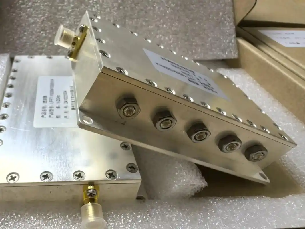
  • Cavity Low Pass Filters: For high‑power radio systems exceeding tens or hundreds of watts, cavity low pass filters are the industry standard. Machined from solid aluminum or copper, these structures feature internal resonant cavities that provide extremely low insertion loss—often under 0.2 dB—alongside power handling reaching hundreds or thousands of watts. While larger and more expensive to manufacture, cavity low pass filter designs deliver the high Q‑factors required for transmitter outputs in telecommunication base stations and television broadcast towers.

Comparing Filter Topologies

Parameter LC Filter Ceramic RF Filter Cavity Low Pass Filter
Frequency Range DC – 1 GHz 300 MHz – 6 GHz 500 MHz – 40 GHz
Insertion Loss 0.5 – 2.0 dB 0.5 – 1.5 dB 0.1 – 0.5 dB
Power Handling < 5 W < 10 W 10 W – 500 W+
Physical Footprint Medium Compact / SMT Large
Relative Cost Low Medium High

Critical RF Filter Specifications Every Engineer Must Evaluate

Matching a filter to a system layout requires reviewing key RF filter specifications. Overlooking a single parameter can cause receiver desensitization, thermal overload, or degraded data throughput.

  • Cutoff Frequency (Fc ): The frequency where signal power drops by 3 dB relative to passband transmission. \(F_c\) marks the upper boundary of usable passband spectrum.
  • Insertion Loss: Attenuation introduced inside the passband. Lower insertion loss preserves power amplifier efficiency and keeps system noise figures down.
  • Stopband Rejection: The depth of attenuation at specific harmonic or interferer frequencies, measured in decibels. This spec determines how effectively the filter blocks out‑of‑band noise.
  • Return Loss and VSWR: Voltage Standing Wave Ratio measures impedance matching across the system's characteristic impedance (typically 50 Ohms). Poor return loss reflects power back toward the transmitter power amplifier, generating heat and distortion.
  • Filter Order and Roll‑off: The number of poles dictates rejection steepness past the cutoff point. A standard 3rd‑order design offers roughly 18 dB per octave roll‑off, whereas a 7th‑order design provides up to 42 dB per octave. Adding poles sharpens roll‑off, but it also increases insertion loss, phase non‑linearity, and circuit size.
  • Group Delay Flatness: In digitally modulated communication setups (such as QAM or OFDM), non‑linear phase response creates delay variations across passband frequencies. Flat group delay limits inter‑symbol interference and keeps bit error rates low.

Real‑World Application and Troubleshooting

In a UHF transmitter redesign operating around 270 MHz, engineers encountered issues with excessive 3rd harmonic emissions at 810 MHz. The legacy surface‑mount LC low pass filter lacked the stopband rejection depth needed to clear FCC compliance standards, exceeding allowable emission limits by 8 dB.

Replacing the discrete LC structure with a high‑Q, 5‑pole ceramic RF filter sharpened the roll‑off curve, pushing harmonic rejection down by an additional 35 dB. This easily brought the transmitter into regulatory compliance. Additionally, switching to the ceramic RF filter's surface‑mount footprint saved board real estate, leaving space for monitoring circuits on the same layer.

Integrating RF Low Pass Filters into Complex RF Systems

Placing an RF low pass filter within the signal chain depends heavily on the operating goals:

  • Transmitter Power Amplifier (PA) Outputs: Positioned immediately following the PA stage, an LPF suppresses high‑power non‑linear harmonics before signals reach the antenna, protecting adjacent channels and keeping transmissions within legal spectral masks.
  • Receiver Front‑Ends: Positioned ahead of low‑noise amplifiers, RF low pass filters prevent high‑amplitude out‑of‑band transmitters from saturating active receiver components.
  • Duplex and Diplexer Assemblies: Combined with high pass or band pass networks, low pass filters separate transmit and receive bands, ensuring clean isolation across shared antenna systems.

Engineering Expertise and Manufacturing Support

Designing high‑performance RF low pass filters requires accurate circuit simulation, custom electro‑magnetic layout tools, and strict production quality control. Modern wireless networks require tailored solutions where off‑the‑shelf components fall short on loss specs or mechanical form factors.

Specialized manufacturers such as Zhenjiang Worldpeak Communication Co., Ltd. support global network rollouts with tailored RF filter engineering. By maintaining fully integrated simulation, prototyping, CNC machining, and automated testing facilities, custom ceramic RF filters and cavity low pass filter assemblies can be tailored to exact system demands. Each filter undergoes full vector network analyzer testing for insertion loss, VSWR, and rejection parameters prior to installation, helping engineers deliver reliable wireless performance worldwide.
Popular News

What environmental resistance can be customized for OEM rf cable

What environmental resistance can be customized for OEM rf cable

2026/09/25

Customize an rf high frequency cable for temperature, moisture, corrosion, vibration, flexing, and OEM validation needs.
How customized coaxial jumper assemblies streamline equipment assembly lines

How customized coaxial jumper assemblies streamline equipment assembly lines

2026/09/25

Streamline RF equipment assembly lines with custom coaxial jumpers. Reduce line-side rework, ensure precise routing, and boost production efficiency.
PL-259 Connector Guide: Installation and RF Applications

PL-259 Connector Guide: Installation and RF Applications

2026/09/25

Learn PL-259 connector selection, soldering, weatherproofing, and RF applications for dependable antenna feedlines.
How to confirm impedance parameters during ODM coaxial adapter development

How to confirm impedance parameters during ODM coaxial adapter development

2026/09/25

Confirm impedance for a 90 degree coax connector with an ODM test plan covering VNA setup, VSWR, acceptance criteria, and release records.
Why anti corrosion treatment is optional for OEM N type connector

Why anti corrosion treatment is optional for OEM N type connector

2026/09/25

Learn when an n type coax connector can omit extra anti-corrosion treatment and when OEM exposure conditions require it.
How sample making process works for ODM custom cable assembly projects

How sample making process works for ODM custom cable assembly projects

2026/09/25

Learn how the custom cable and wire sample process helps ODM buyers validate design, testing, and production readiness.