EN
EN

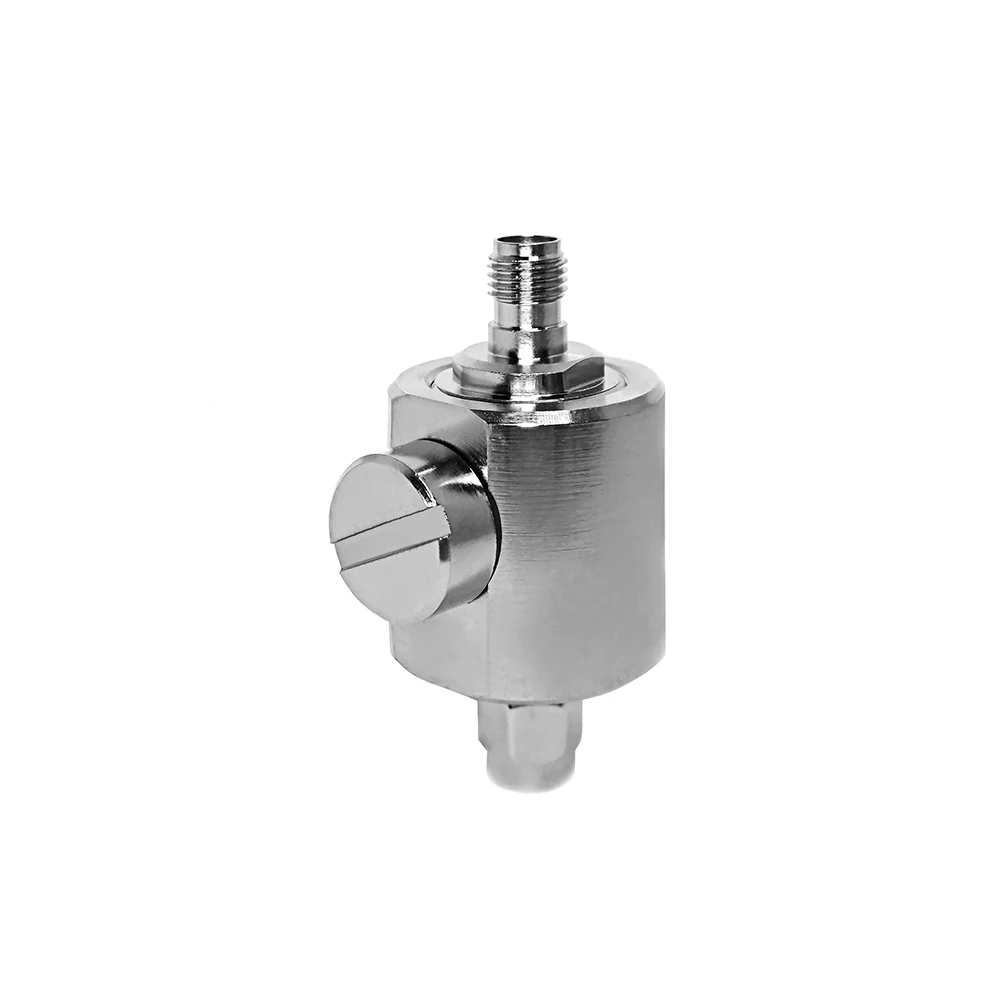
At high frequencies, a connector is far more than a basic mechanical fast-fitter. Components like a right angle SMA connector sit at the precise junction where PCB layout, cable routing, enclosure constraints, soldering workflows, and signal performance intersect. Collaborating with an experienced Original Design Manufacturer (ODM) before freezing a part number helps engineering teams turn a raw schematic concept into a manufacturable, testable, and repeatable production solution.
For hardware engineers building telecom infrastructure, automated test fixtures, industrial control systems, base station antennas, or compact wireless devices, the primary challenge is rarely just physical fit. The true test is whether the entire RF transmission path maintains impedance stability, low insertion loss, and low Voltage Standing Wave Ratio (VSWR) once mass production begins. A disciplined ODM co-design workflow provides a clear, structured review framework to resolve these variables early.
Key Technical Evaluation Areas
-
Signal Path Transitions: Matching PCB trace geometry to internal connector pins.
-
Ground Return via Placement: Minimizing parasitic inductance around the signal launch.
-
Mechanical Interface Clearance: Ensuring enclosure, panel, and cable bend radius fit.
-
Process Compatibility: Validating solder reflow thermal profiles and automated assembly.
Start with System Context Over Catalog Part Numbers
A right angle SMA connector is usually selected when enclosure depth, cable routing angles, or component density makes a straight launch impractical. The initial engineering consultation should evaluate the total operating ecosystem rather than isolated component specs:
-
Frequency Spectrum & Impedance: Target operating bandwidth (e.g., DC to 6 GHz, 18 GHz, or higher) along a controlled 50-ohm transmission line.
-
PCB Stack-Up & Substrate: Dielectric constant, substrate thickness (e.g., FR-4, Rogers), microstrip vs. grounded coplanar waveguide (GCPW) routing.
-
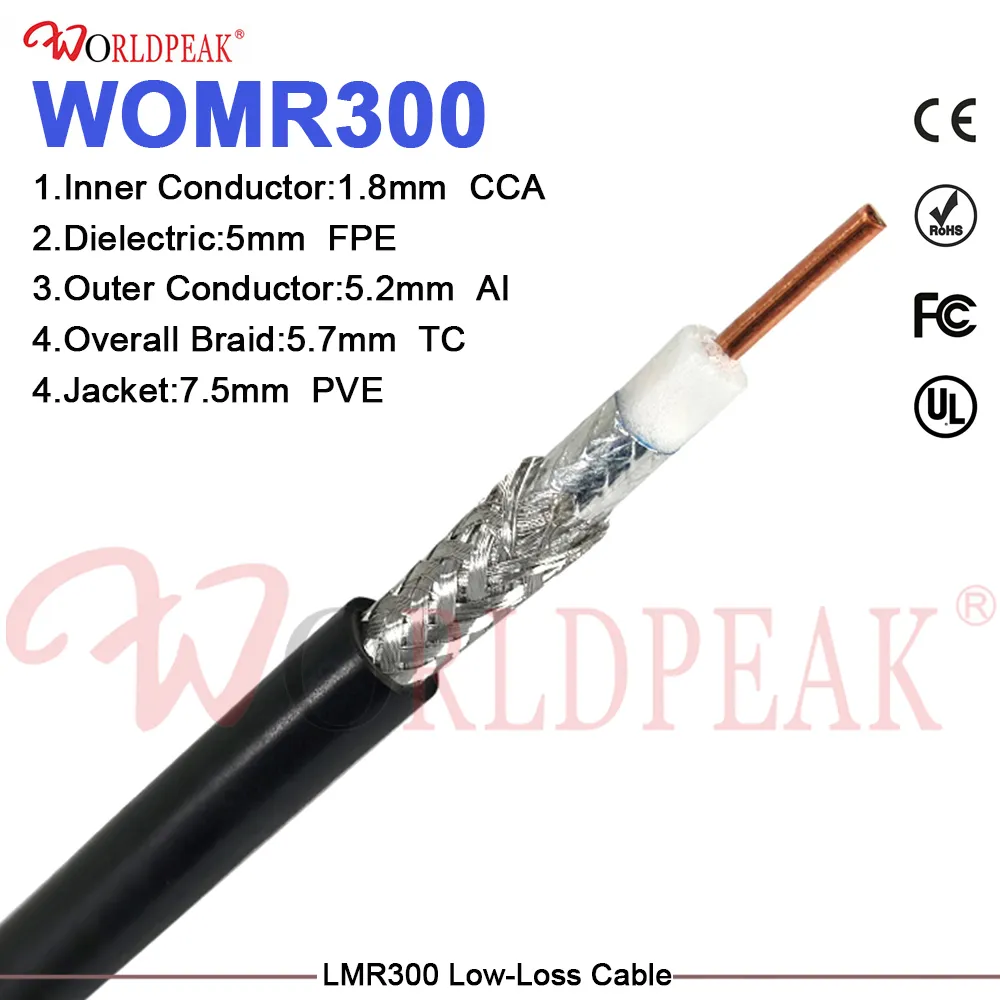
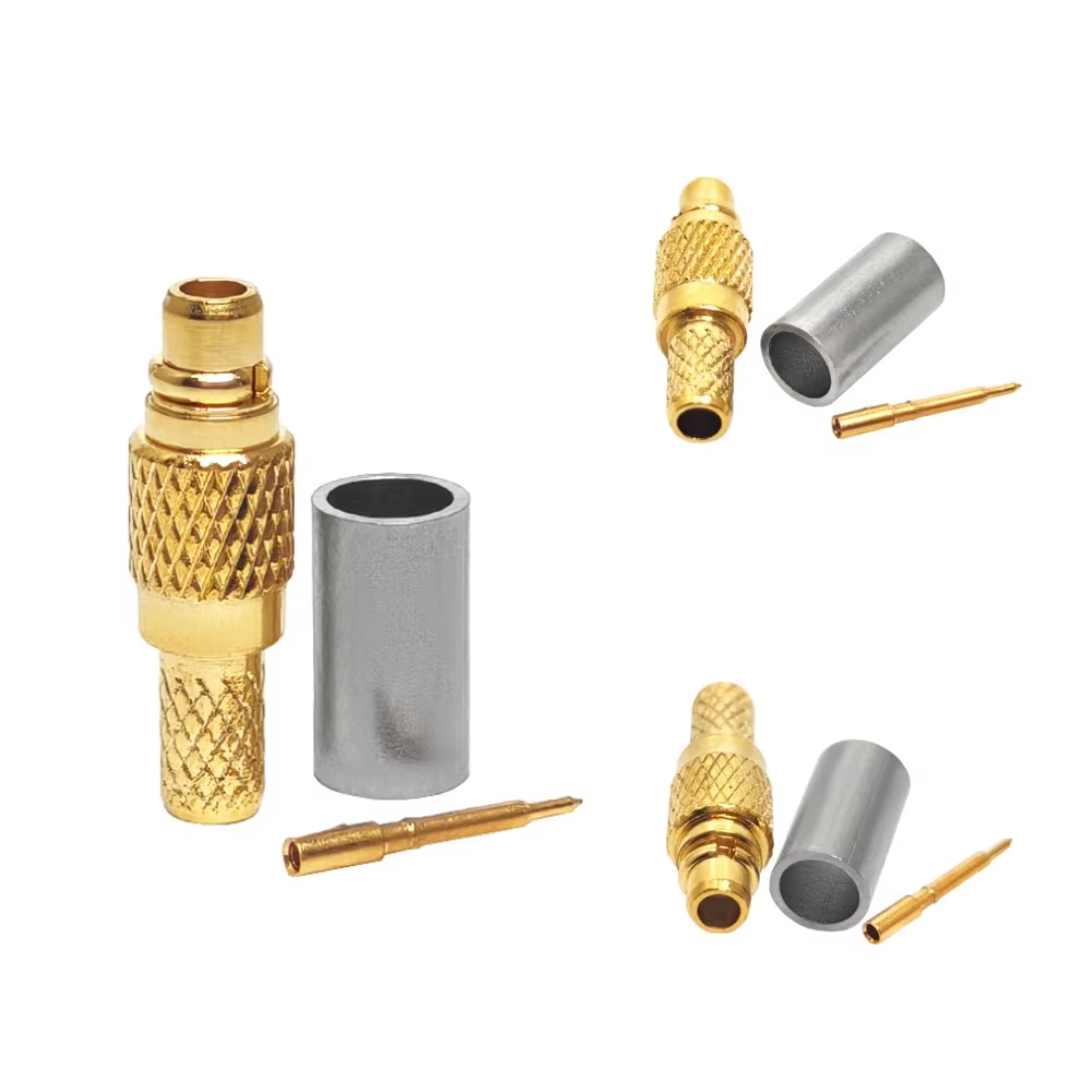
Cable Interface & Termination: Flexible, conformable, or semi-rigid cable types, crimp ferrule vs. direct solder attachment.
-
Enclosure & Environmental Exposure: Panel thickness limits, ingress protection requirements, mechanical shock, and thermal cycling.
Separating fixed mechanical constraints from flexible preferences allows ODM engineers to recommend performance-enhancing design tweaks without compromising core system architecture. Fixed constraints include interface gender, board-edge footprint, anti-rotation panel flats, and mounting holes. Flexible preferences encompass plating options (gold, nickel, or tri-metal), packaging methods, and visual branding.
Translating RF Intent into Interface and PCB Layout Optimization
While SMA interfaces are standardized threaded 50-ohm designs, the physical connector body alone does not guarantee a seamless 50-ohm transition. Integrating a right angle SMA connector introduces internal mechanical right-angle bends that alter center conductor geometry and ground return spacing.
The transition from coaxial geometry to a planar PCB trace requires precise optimization:
-
Pad Dimensions & Cutouts: Adjusting copper ground plane cutouts (ground voiding) directly beneath surface-mount signal pads minimizes parasitic capacitance.
-
Ground Via Fencing: Placing ground vias strategically on both sides of the RF signal pad maintains a continuous ground return path, suppressing unwanted radiation and high-frequency resonances.
-
Solder Volume Control: Excessive solder paste application on the RF pin alters local impedance, causing severe impedance dips at higher frequencies.
An experienced ODM partner conducts joint reviews of mechanical STEP models alongside PCB Gerber/CAD data. Identifying localized impedance discontinuities early prevents costly board spins and delayed product launches.
Critical Pre-Sampling Technical Checklist
To streamline the prototype cycle and avoid late-stage redesigns, clarify these core technical questions prior to sample fabrication:
-
Orientation Reference: Is the right-angle direction defined from the PCB surface, the enclosure wall, or the mating cable exit vector?
-
Mounting Configuration: Will the design utilize an edge-launch, surface-mount (SMT), through-hole, or bulkhead SMA connector mounting style?
-
Ground Return Geometry: Does the PCB layout provide sufficient perimeter grounding around the launcher pin?
-
Mechanical Clearance: Is there adequate clearance for torque wrenches, bulkhead locking nuts, and cable strain-relief boots?
-
Acceptance Criteria: What specific RF sweeps (VSWR, Insertion Loss, Phase Stability) and mechanical tests (pull force, torque resistance) will govern lot approval?
When a bulkhead SMA connector forms part of the outer chassis boundary, it serves a dual role: an RF transition and a mechanical seal. Panel thickness tolerances, O-ring gasket compression, nut tightening torque, and anti-rotation keyways must be evaluated alongside the internal cable-to-board routing to avoid mechanical stress on solder joints.
Prototype Validation and Design for Manufacturability
Prototyping serves as a rigorous engineering validation gateway rather than a routine purchasing check. Production-grade prototypes must mirror the intended mass-production materials, plating specs, internal dielectric insulations, and termination methods.
During prototype evaluation, design teams must assess Design for Manufacturability (DFM) factors:
-
Thermal Mass & Reflow Compatibility: Thicker connector bodies require precise reflow temperature profiling to prevent cold solder joints without melting internal PTFE insulators.
-
Inspection & Solder Joint Access: Solder joints should be easily visible for automated optical inspection (AOI) or manual quality checks.
-
Mechanical Stress Isolation: Tightening a panel nut on a bulkhead SMA connector should not transmit rotational torque or bending stress directly into delicate PCB solder pads.
Small mechanical adjustments at this stage—such as adding mechanical retention legs, optimizing knurling patterns, or tweaking pin contact lengths—dramatically improve long-term joint reliability and production yield.
Building a Controlled Production Approval Package
Before transitioning from validated samples to full-scale volume manufacturing, the ODM partner consolidates all agreed specifications into a controlled production package:
-
Detailed Mechanical Drawings: Interface dimensions, pin tolerances, plating thickness ranges, and surface finishes.
-
Footprint & PCB Guidelines: Recommended copper pad dimensions, solder mask openings, and ground via placement schemas.
-
Testing & Inspection Parameters: In-line VSWR sweep limits, insertion loss thresholds, corrosion testing standards, and mechanical retention specs.
-
Packaging & Handling: Custom tray configurations, tape-and-reel specs, and protective dust cap inclusions.
-
Change Management Protocols: Formal engineering change order (ECO) procedures governing any future material, tooling, or plating modifications.
A transparent ECO process ensures that seemingly minor component substitutions—such as an alternative plating alloy or a dielectric supplier change—are thoroughly re-evaluated before implementation, safeguarding RF path integrity.
Comprehensive Interconnect Engineering and Manufacturing Capabilities
Successfully launching high-frequency wireless products relies on a manufacturing partner capable of converting complex RF requirements into reliable, high-yield components. Modern OEM/ODM interconnect manufacturing demands high-precision CNC machining, strict quality assurance, and comprehensive high-frequency testing infrastructure.
To explore custom RF connector developments, right-angle interface configurations, and precision custom assemblies tailored for demanding communication systems, visit